目录
- 1 Overview
- 2 Display Architectures
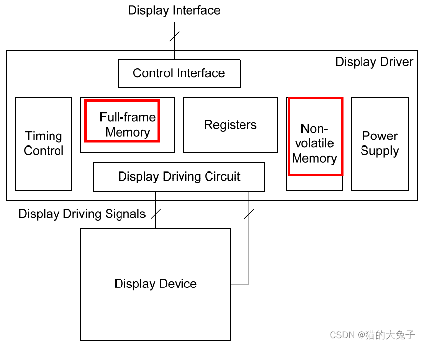
- 2.1 Type 1 Display Architecture Block Diagram
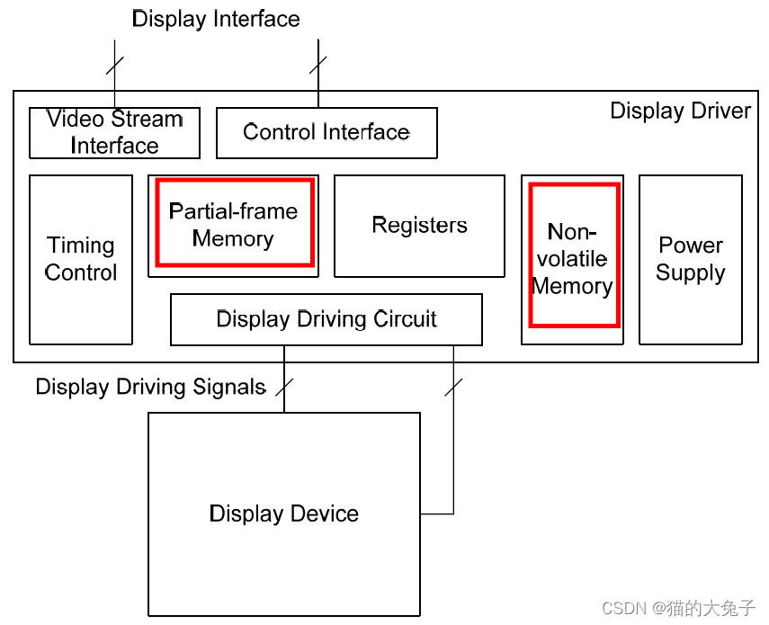
- 2.2 Type 2 Display Architecture Block Diagram
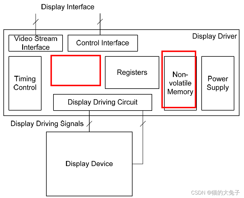
- 2.3 Type 3 Display Architecture Block Diagram
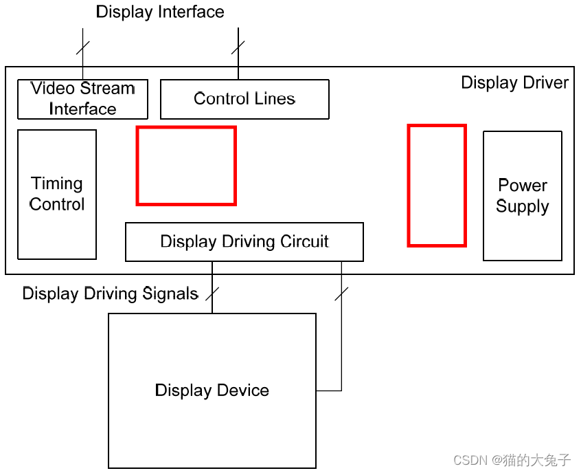
- 2.4 Type 4 Display Architecture Block Diagram
- 3 Interface Signal Description
- 3.1 Power Supply Connections
- 3.2 Interface Signals
- 4 Timing
- 5 Type 4 Architecture Control Command
-
- 5.2 Color Mode
1 Overview
DPI 全称Display Pixel Interface,用于手持设备的有源矩阵 LCD 显示器。 该接口可以配置有 16、18 或 24 个并行数据位的数据路径以及多个控制信号。 DPI采用同步、时钟、数据线等来传输特定图像数据,并采用SPI等其他控制线完成命令控制。在某种程度上,DPI与DBI的区别主要由两点:
- DPI的数据线和控制线分离,而DBI是复用的。
- DPI是实时数据流,显示模块可以不需要内部GRAM,而DBI不是。
DPI直接写屏,速度快,常用于显示视频或动画用,同样缺点也很明显,那就是功耗与带宽。
参考文档:《MIPI Alliance Standard for Display Pixel Interface (DPI-2)》
2 Display Architectures
显示模块应基于如下4种显示架构:
根据是否有帧缓存buffer与寄存器配置存储进行区分
- The Type 1 Display Architecture:
- The Type 2 Display Architecture:
- The Type 3 Display Architecture:
- The Type 4 Display Architecture:
2.1 Type 1 Display Architecture Block Diagram
2.2 Type 2 Display Architecture Block Diagram
2.3 Type 3 Display Architecture Block Diagram
2.4 Type 4 Display Architecture Block Diagram
3 Interface Signal Description
在主处理器和显示模块之间有两种类型的信号连接:
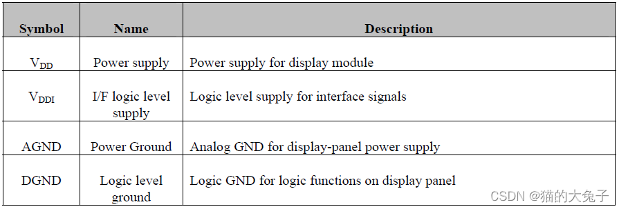
- 电源信号。 电源由主处理器或由主处理器控制的电源管理单元提供。
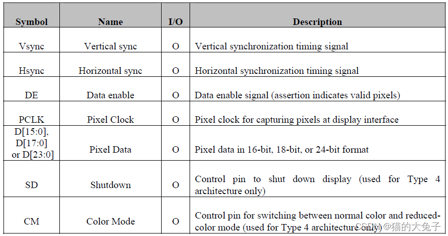
- 接口信号。 使用接口信号在主处理器和显示模块之间传输像素数据、命令和控制信息。
控制信息只能通过CM和SD两根信号线发送Color Mode与Shutdown两种 主处理器应支持 2 类、3 类和 4
类显示架构的所有控制信号。SD 和 CM 是仅符合 4 类标准的显示模块所需的控制信号。
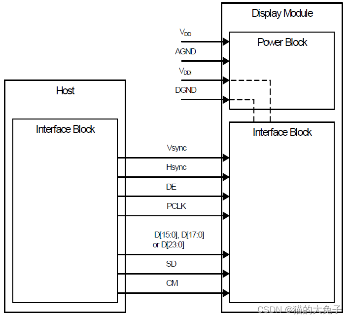
3.1 Power Supply Connections
3.2 Interface Signals
4 Timing
在正常操作中,基于 DPI 架构的系统依靠主机处理器以足够的帧速率连续提供完整的图像数据帧,以避免闪烁或其他可见伪影。显示的图像或帧由像素的矩形阵列组成。 帧作为像素序列从主处理器传输到显示模块,图像数据的每条水平线作为一组连续像素发送。
Vsync 表示显示图像的每一帧的开始。
Hsync 表示每个水平像素行的开始。
每个像素值(16 位、18 位或 24 位数据)在一个像素周期内从主处理器传输到显示模块。 显示模块使用 PCLK 的上升沿来捕获像素数据。 由于 PCLK 连续运行,因此需要控制信号 DE 来指示何时在像素数据信号上传输有效的像素数据。
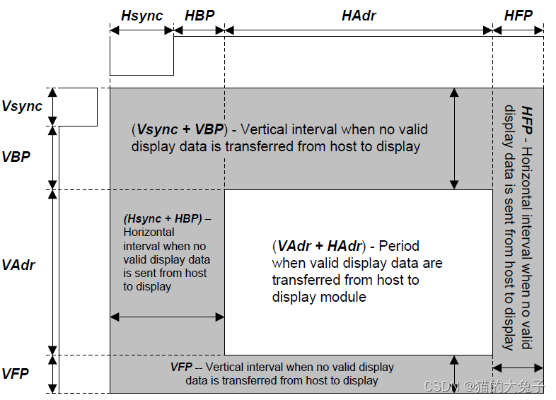
从上图可知,对于DPI timing我们需要配置的时序较多,具体如下图:
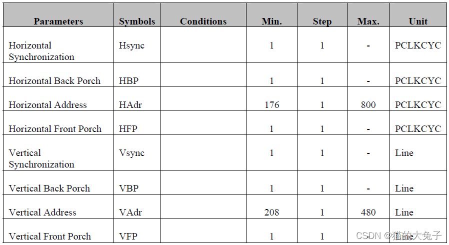
垂直周期(一帧)应等于 Vsync + VBP + VAdr + VFP 之和。
水平周期(一行)应等于 Hsync + HBP +
HAdr + HFP 之和。 在主机处理器和显示模块之间传输有效像素时,控制信号 PCLK 和 Hsync 应始终按规定传输。
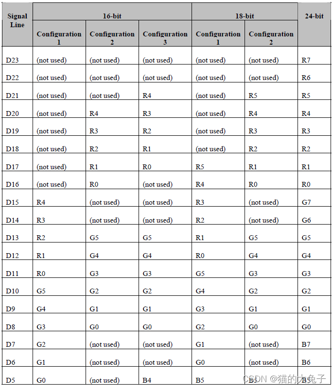
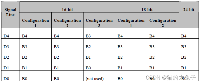
同时,在配置参数时,肯定需要考虑像素的颜色格式:
标准DPI仅支持RGB方式的如下几种颜色格式。
- 16-bit RGB565 option1
- 16-bit RGB565 option2
- 16-bit RGB565 option3
- 18-bit RGB666 option1
- 18-bit RGB666 option2
- 24-bit RGB888
5 Type 4 Architecture Control Command
正如前面提到,在Type 4显示架构上,有两种命令由SD与CM两根信号线控制。
下面分别介绍
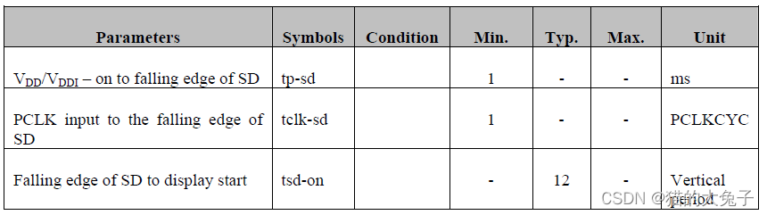
5.1 Shutdown
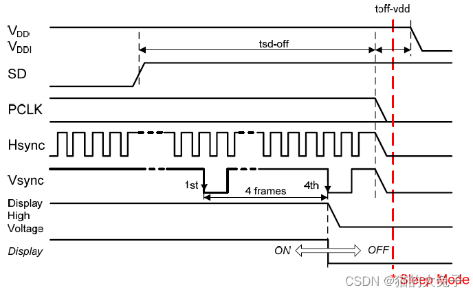
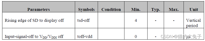
Shutdown信号(SD)用于打开或关闭显示模块。当 SD 为高电平时,主处理器应停止向显示模块传输视频流数据,以降低接口信号功耗。 PCLK 也可以关闭以进一步降低功耗。但显示模块可以通过关闭其内部电路来降低其功耗。 控制接口应保持通电。
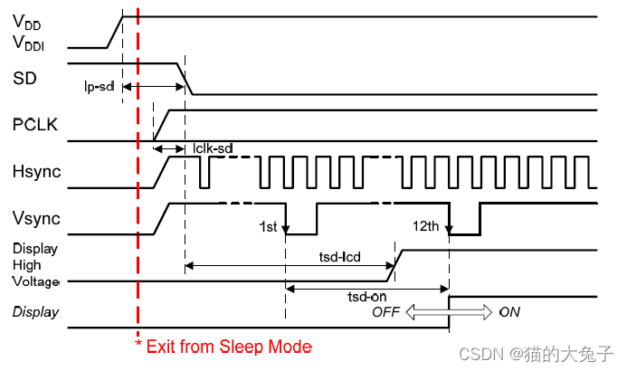
Power-on and Shutdown Recovery Sequence:
Power-off and Shutdown Sequence:
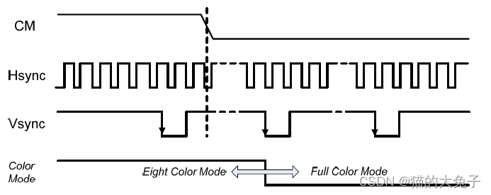
5.2 Color Mode
Color mode信号 CM 用于更改显示的颜色数量。当 CM 为高电平时,显示模块应使用八种颜色显示图像数据,每个 R、G 和 B 颜色分量的 MSB。 可以同时停止显示模块上所有不必要的电路,以降低显示模块的功耗。
Full-color to 8-color Mode Transition Sequence:
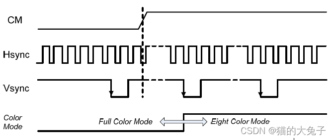
8-color to Full-color Mode Transition Sequence:
本文内容由网友自发贡献,版权归原作者所有,本站不承担相应法律责任。如您发现有涉嫌抄袭侵权的内容,请联系:hwhale#tublm.com(使用前将#替换为@)